
For more than half a century, Moore’s Law has served as the guiding principle of the semiconductor industry — with processor performance doubling every 18–24 months thanks to continuous transistor miniaturization. However, as manufacturing processes approach 2 nm and below, rising costs and physical limitations are gradually slowing down this progress.
Therefore, instead of relying solely on front-end scaling, the global semiconductor industry is now shifting to the back-end — known as Advanced Packaging (AP) — where chip performance is improved by integrating multiple chiplets (logic, memory, analog, and I/O) into a single package.
According to McKinsey (2024), advanced packaging will account for over 50% of total semiconductor industry value growth by 2030, with technologies such as Fan-Out WLP, 2.5D/3D stacking, CoWoS, and Hybrid Bonding becoming the strategic pillars for AI, HPC, and edge computing chips.
⚙️ Highlighted Technologies in Advanced Packaging
| Technology | Description | Typical Applications |
| Fan-Out Wafer-Level Packaging (FOWLP) | Expands interconnect area without using traditional substrates, reducing package thickness and cost. | Smartphones, SoCs, RF modules. |
| 2.5D Integration (Interposer / Bridge) | Uses silicon or glass interposers with RDL to link logic chips and HBM memory, increasing bandwidth and reducing latency. | AI accelerators, HPC GPUs, data center chips. |
| 3D Stacking & Hybrid Bonding | Vertically stacks chips with direct bonding layers, achieving extremely high interconnect density. | HBM3e, CPU–GPU combos, chiplet-based systems. |
(Sources: SEMI Market Intelligence Report 2024; IEEE Spectrum, March 2024)
🌎 A Global Surge of Investment in Packaging Infrastructure
The year 2024 witnessed an unprecedented boom in investments in the advanced packaging sector, with multi-billion-dollar projects launched worldwide — supported by government programs such as the CHIPS Act in the U.S., EU, Japan, and India. This marks how the world is “upgrading” its semiconductor supply chain.
Based on three 2024 reports from the U.S. Department of Commerce CHIPS Office, SEMI, and Bloomberg Semiconductor Insights, some of the most notable projects include:
🔸 United States
- Amkor (Arizona): US $2 billion investment (with $400 million CHIPS Act funding) to build an advanced packaging and testing campus supporting CoWoS and InFO, in collaboration with TSMC.
- SK hynix (Indiana): US $3.87 billion investment to establish an HBM (High Bandwidth Memory) packaging facility.
- NSTC (Tempe, Arizona): A US $1.1 billion national initiative to develop the National Advanced Packaging Piloting Facility.
🔸 Europe and Japan
- ESMC (Dresden) and JASM (Kumamoto): joint ventures among TSMC, Sony, Toyota, and Bosch, receiving billions in subsidies.
- Amkor–Infineon (Portugal) and Merck–DuPont–Fujifilm: focusing on developing advanced materials and equipment for glass substrates and hybrid bonding.
🔸 Asia
- Tata–PSMC (India): US $11 billion investment for the country’s first integrated fab with advanced packaging capabilities.
- Foxconn–HCL and CG Power–Renesas–Stars Microelectronics: establishing OSAT facilities for wire-bond, flip-chip, and SiP processes.
- Toppan (Singapore): US $338 million investment to build a substrate manufacturing plant dedicated to AI packaging.
🧩 “Lab–Fab Integration” — The World’s New Paradigm
Leading nations are promoting the Lab–Fab Integration model, linking research – prototyping – manufacturing (R&D – Pilot – Production) to shorten innovation cycles and accelerate commercialization of new packaging technologies.
Examples include:
- Amkor–TSMC (CoWoS, InFO)
- SK hynix HBM Campus
- ASU–Deca Hub (Fan-Out R&D)
The combination of front-end fabs, back-end OSAT facilities, and design houses (EDA/IP) is forming closed-loop ecosystems, enabling nations to gain greater autonomy and resilience across the semiconductor value chain.
🧩 Da Nang and Vietnam’s First Advanced Packaging Lab-Fab
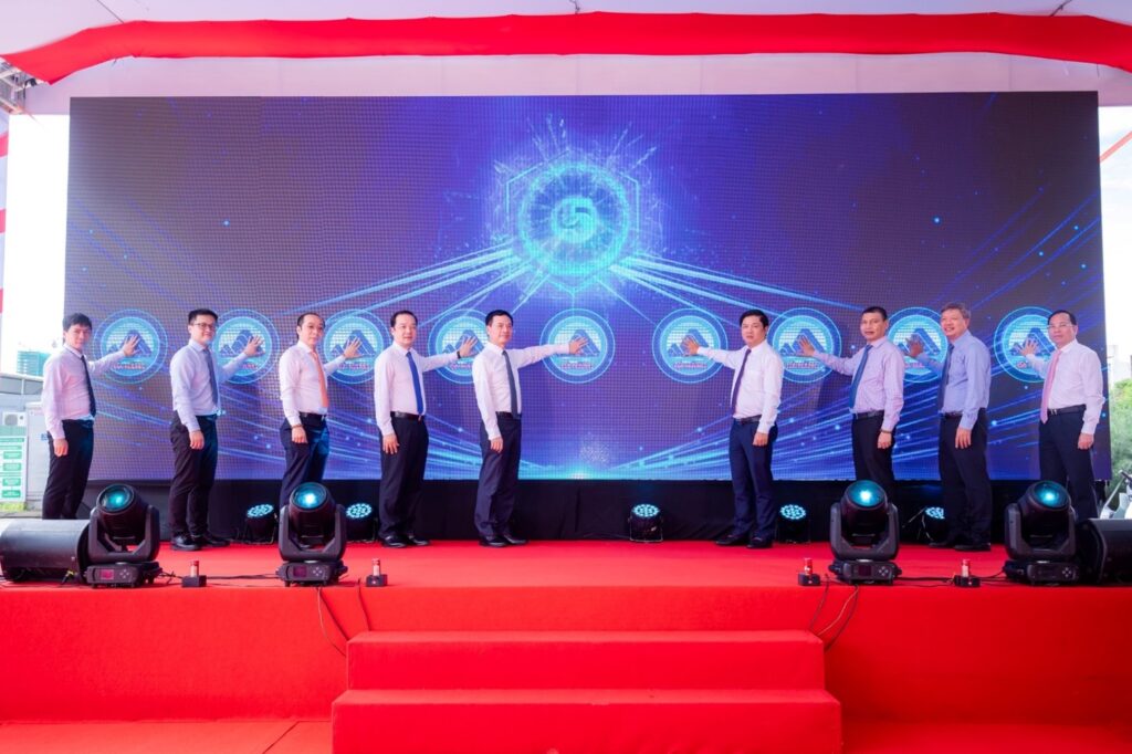
In this global race, the VSAP Lab–Fab project in Da Nang represents a strategic milestone for Vietnam. The facility serves as a center for research, training, and prototyping in advanced semiconductor packaging, contributing to:
- Building Vietnam’s domestic back-end supply chain, enabling deeper participation in the global semiconductor ecosystem.
- Establishing a national R&D and training foundation, where universities, startups, and enterprises can access an internationally standardized environment.
- Attracting foreign investment and technology transfer, acting as a “sandbox” for global collaboration.
- Enhancing technological sovereignty and supply chain resilience, aligning with Vietnam’s national semiconductor strategy (Decision 1018/QĐ-TTg 2024 and Decision 1131/QĐ-TTg 2025).
🧠 Conclusion
From these developments, it is evident that advanced packaging is the “other half” of the semiconductor revolution — where performance comes not only from smaller transistors, but also from how chips interconnect and operate synergistically.
The Lab–Fab project in Da Nang is more than an R&D facility; it represents a transformative step in Vietnam’s semiconductor journey — from assembly to innovation — and a vital contribution toward realizing the vision of “Silicon Bay” in Da Nang.
📚 References
- SEMI Market Intelligence Report: Advanced Packaging Outlook 2024
- IEEE Spectrum, “Why 3D and Fan-Out Packaging Are the Future Beyond Moore’s Law”, March 2024.
- U.S. Department of Commerce – CHIPS for America Press Release, July 2024.
- McKinsey & Company, “Semiconductor Packaging at the Crossroads: 2024 Global Outlook.”
- Bloomberg Intelligence, “Global Semiconductor Supply Chain Reconfiguration, 2024.”
Phuc Le – VSAP Lab
Illustration: Minister of Science and Technology and Da Nang Party Secretary attending the Launch Ceremony of the VSAP Lab–Fab Project on July 28, 2025.


 Tiếng Việt