
For many years, semiconductor packaging was viewed as a “back-end step” — far less glamorous than wafer fabrication or EUV lithography. However, with the rise of AI and high-performance computing, that perception has completely changed. Today, advanced packaging is no longer the final step; it is the strategic chokepoint determining the growth capacity of the entire semiconductor value chain.
The advanced packaging market is growing at 26% annually, heading toward USD 80 billion by 2033, driven by chiplets, multi-die architectures, HBM, and large-scale AI systems. This surge forces the world to rethink:
“It’s not just wafer. It’s not just EUV.
Advanced packaging is now the biggest bottleneck.”
1) Asia – the U.S. – Japan: Three Completely Different Strategies
Asia: Still the world’s “semiconductor packaging factory”
South Korea, Taiwan, and China continue to dominate OSAT and advanced packaging:
- South Korea: accelerating HBM, the strongest capability globally.
- Taiwan: TSMC leads in CoWoS but is severely capacity-constrained (6–9 months backlog).
- China: pushing localization, focusing on 2.5D, 3DIC, and investing heavily in module packaging to reduce foreign dependence.
- Asia’s advantages: complete supply chains, large labor force, and decades of operational expertise.
United States: From lagging behind to determined reinvestment
The U.S. has realized that advanced packaging — not chip fabrication alone — is its critical strategic weakness. Today, the U.S. is:
- Investing CHIPS Act funding into the national advanced packaging centers
- Building new advanced packaging fabs by Amkor, Intel, and federal R&D hubs
- Rapidly expanding workforce development in packaging — historically its weakest link
Long-term goal: rebuild domestic advanced packaging capability, reduce dependence on Asia, and secure the defense-AI supply chain.
Japan: A disciplined, methodical comeback
Japan is returning to the game with a structured strategy:
- Increasing investment in wafers, materials, substrates, epoxy, and tools — areas of traditional Japanese strength
- Attracting TSMC’s Kumamoto project and follow-on phases
- Revitalizing its domestic packaging ecosystem and linking it with automotive, electronics, and equipment industries
Japan is rebuilding a “complete value chain” to gain advantage in quality and reliability.
2) The Unresolved Bottlenecks — Despite Explosive Demand
AI companies are racing to build larger models, but system production is slowing down due to packaging constraints:
- CoWoS / 2.5D capacity cannot meet demand from NVIDIA, AMD, Broadcom, and Marvell — customers wait months for interposers, an unprecedented situation in semiconductor history.
- HBM is absorbing global resources: TSV, stacking, testing, and yield remain critical bottlenecks.
HBM demand has increased 4–6× within just two years. No supplier can keep up. - Shortage of T-glass core for high-end substrates: Japan, Korea, and Taiwan all lack sufficient T-glass manufacturing capacity, causing chronic substrate bottlenecks.
- Global packaging talent crisis: bonding, lithography, and test engineers are in extreme shortage. This will be a structural risk for the entire decade ahead.
- Advanced packaging equipment scarcity: bonding tools, lithography, curing systems, and inspection machines now require 9–18 months lead time.
3) Advanced Packaging – The “New ASML” of the AI Era
In the chiplet era, advanced packaging is no longer a simple back-end process. It has become a high-precision, technology-intensive domain requiring complex equipment, specialized materials, and deep expertise.
Advanced packaging now encompasses:
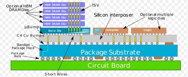
- 2.5D / 3DIC
- Hybrid bonding
- Chiplet integration
- High-density substrates
- Advanced thermal management
- HBM stacking
This is an entirely new technology race.
4) A Strategic Outlook for the Next Decade
“The next decade will not be determined by how many EUV scanners a country owns —
but by what happens inside advanced packaging factories.
Whoever resolves the packaging bottlenecks first will dominate the AI era.”
Advanced packaging is not a short-term trend. It is the core battleground of the semiconductor industry for the next 10–15 years.
(Tien Duong)

 Tiếng Việt